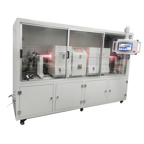
Atomic Layer Deposition (ALD) System – Precision Thin Film Engineering at the Atomic Scale
Overview
Le Atomic Layer Deposition (ALD) System is a cutting-edge thin-film deposition technology that enables the growth of ultra-thin, conformal, and highly uniform films with atomic-level precision. Unlike traditional CVD or PVD methods, ALD operates through a self-limiting surface reaction mechanism, allowing precise control over film thickness down to sub-nanometer resolution.
This system is ideal for advanced applications in semiconductors, microelectronics, energy storage, biomedical devices, and nanotechnology, where uniformity, pinhole-free coverage, and high purity are critical.
Our ALD system supports a wide range of materials—including oxides, nitrides, metals, and complex compounds—making it a versatile platform for both research and industrial production.
How It Works: The Principle of ALD
Atomic Layer Deposition is based on sequential, self-saturating surface reactions between two or more chemical precursors. The process follows four key steps:
- Pulse 1: A precursor gas (e.g., TMA for Al₂O₃) is introduced into the chamber and adsorbs onto the substrate surface.
- Purge: Inert gas (e.g., N₂ or Ar) removes excess precursor and byproducts.
- Pulse 2: A second precursor (e.g., H₂O) reacts with the first to form a chemically bonded layer.
- Purge: Another purge step removes unreacted species and byproducts.
This cycle repeats until the desired film thickness is achieved. Each cycle deposits one atomic layer, enabling precise thickness control with excellent step coverage even on high-aspect-ratio structures.
Key Applications
| Industry | Application |
|---|---|
| Semiconductors | High-k dielectric layers (HfO₂, Al₂O₃), gate stack engineering, DRAM capacitors |
| Nanoelectronics | Conformal coating of nanowires, 3D NAND memory, FinFETs |
| Energy Storage | Electrode passivation layers for batteries, solid-state electrolytes |
| Photovoltaics | Anti-reflective coatings, transparent conductive oxides (TCOs) |
| Biomedical Devices | Biocompatible coatings (e.g., TiO₂, ZnO), drug delivery systems |
| MEMS & Sensors | Protective layers, functional surfaces for gas/chemical sensing |
| Research & Development | Synthesis of novel materials, quantum dots, heterostructures |
✅ Note: ALD is also used in plasma-enhanced ALD (PE-ALD) and remote plasma ALD for low-temperature processing.
Materials Supported
Our ALD system supports a broad range of metallic, oxide, nitride, and composite materialsy compris :
| Material Class | Examples |
|---|---|
| Oxides | Al₂O₃, TiO₂, ZrO₂, HfO₂, Ta₂O₅, SiO₂, Nb₂O₅, MgO, CaO, CuO |
| Nitrides | AlN, TiN, Si₃N₄, TaN, WN |
| Metals | Ru, Pt, Ir, Pd, Ni, Cu |
| Carbides | TiC, TaC, WC |
| Hydroxyapatite | Ca₁₀(PO₄)₆(OH)₂ (for biomedical implants) |
| Polymers | PMDA–DAH, PMDA–ODA (for organic electronics) |
| Complex Structures | Multilayers, doped films, graded compositions |
🔬 Custom precursor compatibility available upon request.
Avantages techniques
- ✅ Atomic-Level Control: Deposit films with sub-nm precision — perfect for next-gen devices.
- ✅ Excellent Conformality: Uniform coverage on trenches, vias, and 3D structures.
- ✅ High Purity & Low Defects: Self-limiting reactions minimize defects and pinholes.
- ✅ Low-Temperature Processing: Compatible with temperature-sensitive substrates (e.g., polymers, flexible electronics).
- ✅ Scalable Design: From lab-scale R&D to pilot production lines.
- ✅ Modular Architecture: Supports multiple precursors, gas injection modes, and process configurations.
Product Specifications
| Parameter | Specification |
|---|---|
| Deposition Method | Thermal ALD / Plasma-Enhanced ALD (PE-ALD) |
| Temperature Range | 50°C – 400°C (upgradable to 600°C) |
| Chamber Pressure | 0.1 – 100 Torr (adjustable) |
| Precursor Lines | 2–8 channels (configurable) |
| Gas Delivery | Mass flow controllers (MFCs), pulse valves, purging system |
| Control Interface | Touchscreen HMI + PLC logic |
| Contrôle des processus | Automated cycle programming (pulse/purge duration) |
| Vacuum System | Rotary vane pump + optional turbo pump |
| Substrate Size | Up to 6″ wafer or custom holder |
| Rotation Support | Optional rotating stage for improved uniformity |
| Data Logging | Real-time monitoring, cloud storage (optional) |
| Dimensions (L×W×H) | ~1000 × 800 × 1200 mm |
| Weight | ~200 kg |
| Certifications | CE, RoHS, ISO 9001 |
📌 Custom configurations available for specific materials, throughput, or integration with other tools (e.g., sputtering, etching).
Intelligent Features
- Automated Pulse Sequencing:
Pre-programmable cycles with adjustable pulse and purge times for different materials. - Multi-Precursor Support:
Simultaneous or sequential use of up to 8 precursors for complex multilayer films. - Plasma Enhancement Option:
Enables low-temperature ALD using remote plasma source (e.g., O₂, N₂, NH₃). - Remote Monitoring & Cloud Access:
Real-time data logging and remote control via secure network connection. - Over-Pressure Protection:
Automatic shutdown if pressure exceeds safe limits. - Material Library:
Built-in database of common ALD recipes (Al₂O₃, TiO₂, HfO₂, etc.) for quick setup.
Why Choose Our ALD System?
- ✔️ Industry-Leading Precision: Achieve ±1 Å thickness control — essential for advanced device fabrication.
- ✔️ High Throughput & Reliability: Optimized gas dynamics and thermal stability ensure consistent performance.
- ✔️ Flexible Platform: Supports both thermal and plasma-enhanced ALD processes.
- ✔️ Scalable for Production: Designed for seamless integration into semiconductor fabs and R&D labs.
- ✔️ Compliant with Cleanroom Standards: Suitable for Class 100–1000 environments.
Case Study: High-k Dielectric Growth for NAND Flash
A leading memory manufacturer adopted our ALD system to deposit HfO₂ as a high-k dielectric layer in 3D NAND flash memory. Results showed:
- <±2% thickness variation across 300mm wafers
- Perfect conformality in deep-trench structures
- Improved leakage current performance due to defect-free films
This case highlights how ALD enables next-generation scaling in semiconductor manufacturing.
Conclusion
Le Atomic Layer Deposition (ALD) System represents the pinnacle of precision thin-film technology. With its ability to grow atomically controlled, conformal, and ultra-pure films, it is indispensable for pushing the boundaries of nanoelectronics, energy, and biomedicine.
Whether you’re developing advanced memory devices, designing bio-compatible coatings, or exploring new materials, our ALD system delivers unmatched accuracy, reliability, and versatility.
📞 Contact Us Today for a technical consultation, demo, or custom solution design.