Magnetron Sputtering Deposition System – Compact & High-Precision Thin Film Coating Solution
Overview
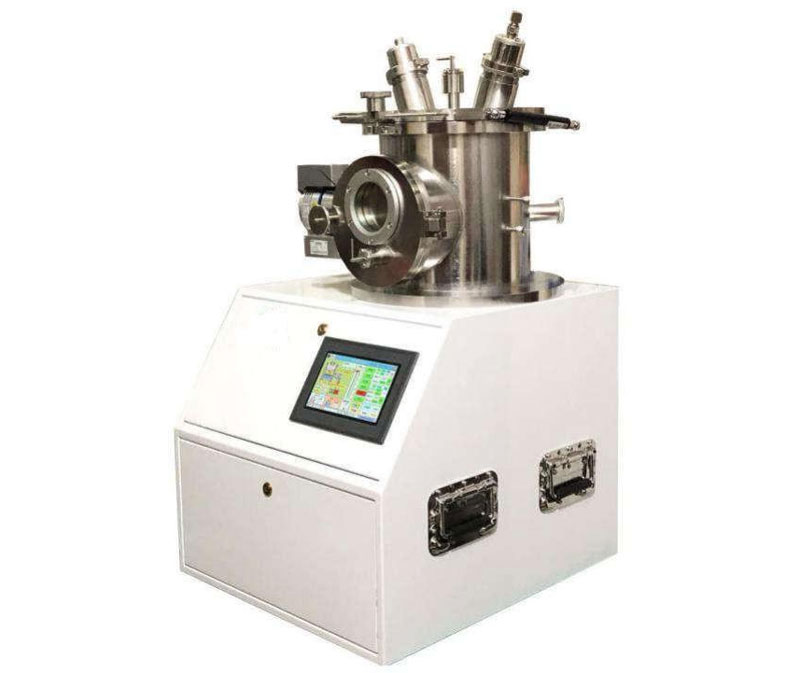
The Magnetron Sputtering Deposition System is a compact, high-performance thin film deposition instrument designed for laboratory-scale research and development in materials science, semiconductor technology, optoelectronics, and surface engineering. This system utilizes DC/RF magnetron sputtering to deposit high-purity, dense, and uniform films from metallic, ceramic, or compound targets under controlled vacuum conditions.
Ideal for fabricating metal electrodes, dielectric layers, transparent conductive oxides (TCOs), and nanostructured thin films, this system is widely used in OLED, OPV, perovskite solar cells, microelectronics, sensors, and functional coatings research.
With its small footprint, low power consumption, and intelligent control system, it is perfectly suited for installation in gloveboxes, fume hoods, or standard lab benches, making it an essential tool for academic and industrial R&D labs.
Caratteristiche principali
- ✅ Compact Design:
Small size (L60×W60×H96 cm) allows placement in confined spaces such as gloveboxes or cleanroom benches. - ✅ Low Power Consumption:
Designed for energy efficiency—ideal for labs with limited electrical capacity. - ✅ High Stability & Reliability:
Uses imported or domestically optimized components (e.g., vacuum pumps, vacuum gauges) to ensure long-term stability and minimal downtime. - ✅ Smart Control System:
PLC + touchscreen intelligent control interface with automatic leak detection, fault alerts, and one-button vacuum shutdown for enhanced safety and ease of use. - ✅ Dual Magnetron Configuration:
Equipped with two 2-inch DC magnetrons (with shutter), optionally upgradable to three sources. Supports both DC and RF power supply, enabling sputtering of conducting and insulating materials. - ✅ Versatile Target Compatibility:
Compatible with metallic (Al, Cr, Ti, Ag, Au), ceramic (SiO₂, Al₂O₃, TiO₂), and compound (ITO, ZnO) targets. - ✅ Vacuum Compatibility:
Achieves base pressure of 8×10⁻⁵ Pa (equivalent to 6×10⁻⁷ Torr) with mechanical + molecular pump configuration. - ✅ Film Thickness Monitoring:
Optional imported or domestic quartz crystal thickness monitor enables real-time monitoring and control of deposition rate and film thickness. - ✅ Rotatable Substrate Holder:
Φ100 mm substrate holder with adjustable rotation speed (0–20 rpm) and temperature control up to 300°C, ensuring uniform coating on various substrates. - ✅ Water Cooling System:
Integrated water-cooled target and chamber shielding prevent overheating and improve sputtering efficiency. - ✅ Flexible Power Supply Options:
- DC pulsed power for metal targets (e.g., Al, Ag)
- RF matching power for insulating materials (e.g., ITO, SiO₂)
- Full automatic impedance matching ensures stable plasma discharge.
Specifiche tecniche
| Parameter | Specification |
|---|---|
| Materiale della camera | 1Cr18Ni9Ti stainless steel, welded structure, double sealing ring design |
| Dimensione della camera | Ø180 mm × 300 mm |
| Vacuum System | Mechanical pump + diffusion/molecular pump (domestic or imported optional) • Base pressure: <8×10⁻⁵ Pa • Pumping speed: 24 L/s • Vacuum gauge: Capacitance manometer (range: 8×10⁻¹⁰ Pa) • Valves: Electromagnetic valve + manual throttle valve |
| Sputtering System | Two 2-inch DC magnetrons (with shutter), upgradeable to three • Water-cooled target holders • DC pulse power (for metals) • RF matching power (for dielectrics) • Automatic impedance matching |
| Substrate Holder | Φ100 mm, height adjustable: 60–120 mm, rotation speed: 0–20 rpm • Heating capability: up to 300°C • Optional bias voltage and ultrasonic cleaning function |
| Thickness Monitor | Optional quartz crystal oscillator (in-situ monitoring of deposition rate and total thickness) |
| Sistema di controllo | PLC + touch screen intelligent control system • Automatic leak detection • Fault diagnosis and alarm • One-key vacuum stop |
| Dimensions (L×W×H) | 60 cm × 60 cm × 96 cm |
| Power Supply | 220V / 380V AC, 50Hz |
| Weight | ~85 kg |
| Interface | Pre-installed CF35 flange port for integration with other systems |
📌 Custom configurations available for larger chamber, multi-source setups, or integration with glovebox systems.
Applicazioni
| Field | Application |
|---|---|
| Organic Electronics | Electrode deposition for OLED, OPV, and OFET devices |
| Photovoltaics | Transparent conductive oxide (TCO) layer coating, back contact formation |
| Semiconductors | Metal gate deposition, interconnect layers |
| Surface Engineering | Functional coatings for sensors, MEMS, and biomedical devices |
| Research & Development | Thin film growth for material characterization, device prototyping |
Why Choose Our Magnetron Sputtering System?
- ✔️ Space-Saving Design: Fits easily into gloveboxes or small lab spaces.
- ✔️ High Precision & Reproducibility: Stable vacuum and temperature control ensure consistent results.
- ✔️ User-Friendly Operation: Touchscreen interface simplifies setup and monitoring.
- ✔️ Safety First: Built-in leak detection and automatic shutdown reduce risks.
- ✔️ Cost-Effective: Lower operating cost compared to large-scale PVD systems.
- ✔️ Flexible Configuration: Supports both metallic and insulating materials.
Case Study: ITO Transparent Electrode Fabrication
A university research team used our magnetron sputtering system to deposit indium tin oxide (ITO) films for transparent electrode applications in flexible solar cells. Results showed:
- High transmittance (>85%) in visible range
- Low sheet resistance (<100 Ω/sq)
- Excellent adhesion and uniformity across 2-inch substrates
- Compatibility with roll-to-roll processing simulation
This enabled rapid prototyping of transparent conductive layers without requiring large-scale equipment.
This case demonstrates how the system supports advanced optoelectronic research with minimal infrastructure investment.
Conclusion
The Magnetron Sputtering Deposition System offers a compact, reliable, and high-performance solution for thin film deposition in academic and industrial laboratories. With its dual magnetron configuration, smart control system, and flexible power options, it delivers excellent film quality and process consistency at an affordable cost.
Whether you’re developing next-generation solar cells, OLED displays, or functional coatings, this system provides the precision, flexibility, and reliability needed for successful R&D.
📞 Contact Us Today for a technical consultation, demo, or custom configuration.