RF Vacuum Plasma Cleaning System – Advanced Dry Etching & Surface Activation for Next-Gen Manufacturing
Introduction: The Evolution of Precision Surface Engineering
In the era of miniaturization and high-reliability electronics, traditional wet cleaning methods are no longer sufficient. Chemical solvents leave residues, mechanical abrasion risks surface damage, and thermal processes can degrade sensitive materials.
The RF Vacuum Plasma Cleaning System represents a breakthrough in dry, non-contact surface treatment technology, offering an environmentally friendly, repeatable, and highly effective alternative for removing contaminants at the molecular level.
Powered by 13.56 MHz radio frequency (RF) energy, this system generates a low-pressure plasma environment that enables deep penetration into microstructures—ideal for semiconductor fabrication, medical device sterilization, and advanced material processing.
Core Technology: How RF Plasma Cleans Surfaces
🔬 Plasma Chemistry in Action
Plasma is created by ionizing gases (e.g., O₂, Ar, N₂) under vacuum conditions using RF power. The process involves:
- Vacuum Environment: Chamber pressure reduced to 10–100 mTorr, minimizing collisions and increasing mean free path.
- RF Excitation: 13.56 MHz AC voltage applied across electrodes or antenna induces electron acceleration.
- Ionization & Reaction: Electrons collide with gas molecules, producing reactive species such as:
- Oxygen radicals (O•) → oxidize hydrocarbons
- Fluorine ions (F⁺) → etch silicon oxides
- UV photons → break molecular bonds
- Volatilization: Contaminants are converted into gaseous byproducts (CO₂, H₂O, etc.) and pumped away.
This chemical + physical dual mechanism ensures thorough cleaning without leaving behind any residue.
Key Applications Across Industries
| Industry | Application |
|---|---|
| Semiconductors | Wafer pre-cleaning before photolithography, native oxide removal, dielectric layer activation |
| PCB & Electronics | Solder mask residue removal, flux cleaning, gold plating pre-treatment, COG/COF bonding prep |
| Medical Devices | Sterilization of implants, catheters, and surgical tools; surface activation for biocompatibility |
| Optoelectronics | LCD/OLED panel cleaning, touch screen (TP) pre-bonding, LED chip surface treatment |
| Advanced Materials | Functionalization of polymers, ceramics, metals, and composites for improved adhesion |
| Research & Development | Surface analysis, nanomaterial synthesis, thin-film deposition support |
✅ Note: This system is also ideal for in-situ cleaning in vacuum coating lines (e.g., PVD, ALD), where contamination control is critical.
Technical Highlights: Why Choose Our RF Plasma Cleaner?
🛠️ 1. High-Frequency RF Power (13.56 MHz)
Standardized frequency used globally in semiconductor and aerospace industries. Ensures stable plasma ignition and uniform energy distribution.
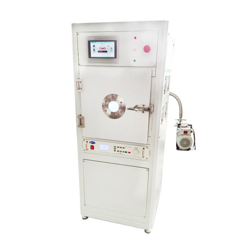
🔧 2. Stainless Steel Chamber (304/316L)
Corrosion-resistant, durable construction designed for long-term operation in aggressive environments.
⚙️ 3. Smart Control System
- Manual Mode: Full operator control over time, power, and gas flow.
- Auto Mode: Pre-programmed sequences with multiple stages (e.g., 2x cleaning cycles).
- Timer Function: Automatic shutdown after preset duration.
💡 4. Advanced Gas Delivery System
- Mass Flow Controllers (MFCs): Precise regulation of gas ratios (e.g., O₂:Ar = 1:1) for optimized cleaning profiles.
- Dual Gas Input: Supports mixed gas plasmas for tailored chemical reactions.
📏 5. Pressure Stabilization (Optional)
Maintains constant chamber pressure during process, ensuring consistent plasma density and cleaning efficiency.
🌐 6. Vacuum Compatibility
Integrates seamlessly with other vacuum systems such as evaporation, sputtering, and lithography tools.
Product Specifications
| Parameter | Specification |
|---|---|
| Power Supply | 13.56 MHz RF Generator |
| Plasma Power | 100W – 2000W (adjustable) |
| Operating Pressure | 10 mTorr – 100 mTorr (adjustable) |
| 챔버 재질 | Stainless Steel (304/316L) |
| Gas Input | O₂, Ar, N₂, H₂, CF₄, SF₆ (optional mixtures) |
| Vacuum Pump | Rotary vane pump or turbo molecular pump (optional) |
| Control Interface | Touchscreen HMI with PLC logic |
| Operation Modes | Manual / Automatic / Smart Auto Mode |
| Timer Function | Programmable cleaning duration (1–9999 seconds) |
| Gas Flow Control | MFCs for precise regulation |
| Pressure Control | Optional auto-pressure stabilization |
| Dimensions (L×W×H) | ~800 × 600 × 1000 mm (standard model) |
| Weight | ~150 kg |
| Certifications | CE, RoHS, ISO 9001 |
📌 Custom configurations available for batch processing, inline integration, or R&D labs.
Environmental & Safety Benefits
- ✅ Zero Liquid Waste: No chemical solvents required → reduces environmental impact.
- ✅ No Secondary Pollution: Byproducts are fully evacuated via vacuum system.
- ✅ Non-Destructive Process: No mechanical stress or thermal damage to substrates.
- ✅ Safe Operation: Enclosed chamber design prevents exposure to plasma and reactive gases.
Case Study: Semiconductor Wafer Cleaning
A leading foundry implemented our RF plasma cleaner in their pre-lithography process line. Results showed:
- 99.9% reduction in organic contamination
- Improved yield by 12% due to fewer defects
- Reduced cleaning time from 30 minutes (wet method) to 5 minutes (plasma)
- Elimination of solvent handling and disposal costs
This case highlights how plasma cleaning not only improves quality but also enhances productivity and sustainability.
Future Outlook: From Cleaning to Functionalization
Beyond cleaning, RF plasma systems are evolving into multi-functional platforms capable of:
- Surface activation for better adhesion
- Etching for micro-patterning
- Deposition of thin functional layers
- Sterilization without heat
As industries move toward smart manufacturing and green chemistry, the RF vacuum plasma cleaner will play a pivotal role in enabling cleaner, faster, and smarter production processes.
Conclusion
The RF Vacuum Plasma Cleaning System is more than just a cleaning tool—it’s a platform for precision surface engineering. With its combination of advanced RF technology, intelligent controls, and industry-proven performance, it sets a new benchmark for surface preparation in high-tech manufacturing.
Whether you’re working in semiconductors, medical devices, or next-gen displays, our system delivers unmatched cleanliness, reliability, and scalability—ensuring your products meet the highest standards of quality and performance.
📞 Contact Us Today for a technical consultation, on-site demonstration, or custom solution design.